Organisational
Faculty: Engineering and Natural Sciences
Location: 14-B008
Phone: +49 (0) 3375 / 508 -
Infrastructure
Work places: 2
Equipment:
-
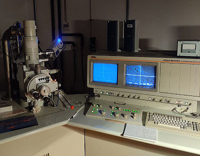
Scanning elctron microscope Jeol JSM-6400
- Energy-dispersive X-ray spectroscope Oxford Instruments
The scanning electron microscope with energy dispersive X-ray spectrometer enables
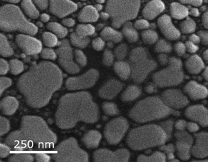
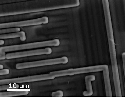
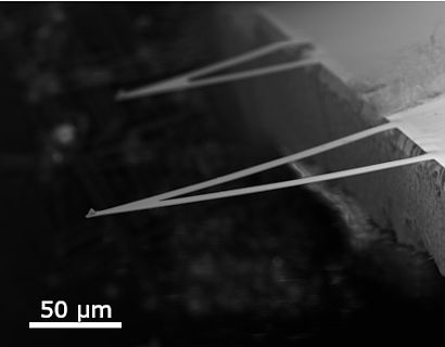
- imaging of the sample surface (topography and atomic number contrast) with very high spatial resolution and depth of field
- chemical analysis.
MethodsOpen areaClose area
In the scanning electron microscope (SEM), the image of the sample surface is created by scanning with a focused high-energy (keV) primary electron beam and detecting secondary electrons or backscattered electrons. By scanning areas of different size on the surface, which are imaged on the same screen size, the magnification changes.
While the detection of secondary electrons (E < 50 eV) provides the best possible spatial resolution, segment detectors for backscattered electrons are used to separate topography from chemical (atomic number) contrast.
The energy of the primary electrons is also sufficient to ionise atoms by knocking out core-level electrons. The resulting core hole is filled by an electron from a higher energy state. The energy difference can be transferred to another electron leaving the material (Auger-Meitner effect, cf. AES) or in form of a photon. The latter is used in energy-dispersive X-ray spectroscopy (EDS or EDX) for a chemical analysis of the sample.
Specifications SEMOpen areaClose area
- Magnification up to 300000x, spatial resolution up to 3.5 nm
- Everhart-Thornley detector for secondary electrons
- Semiconductor segment detector for backscattered electrons
- Sample load lock
- X, Y, Z shift, rotation (0 - 360°) and tilt (-5 - 90°)


