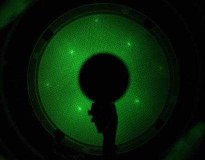
Low-energy electron diffraction (LEED)
Diffraction of low-energy electrons (20 - 200eV) is used to investigate
- symmetry and in-plane lattice constants of the surface
- surface roughness
Funded by the European Union as part of the European Regional Development Fund (ERDF) Infrastructure for Research, Development and Innovation (InfraFEI) programme. Details can be found on the project website InfraMOCha.
MethodOpen areaClose area
The diffraction pattern of low-energy electrons (20 - 200eV) on a luminescent screen is a map of the sample surface in reciprocal space and can be used to determine the symmetry and in-plane lattice constants of the surface. A more accurate determination of atomic positions at the surface including information about the out-of-plane lattice constant can be obtained by measuring the energy-dependent intensity of the diffraction spots (I-V LEED) and compare it to calculated I-V curves.
SpecificationsOpen areaClose area
- µ-metal shielding
- 4-grid-LEED optics in Reverse View Design
- Electron source: light-shielded miniature electron source with Thoria-coated Ir hairpin filament
- Primary energy: up to 1keV
- Spot size: down to < 1mm
- Screen material: glas, with conductive layer of ITO und P43 cadmium-free phosphorus
